

 จองคิวบริการ
 NR tours
 NR shop
 NR jobs
 facebook th
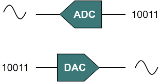
Aerospace and defense frameworks are undergoing a sweeping digital transformation characterized by the rapid replacement of legacy analog heterodyne architectures with direct RF sampling configurations that minimize physical weight and maximize operational flexibility. Modern radar systems, electronic warfare suites, and unmanned aerial vehicle navigation arrays require the instantaneous capture of massive spectral windows to detect low-observability threats and counter sophisticated jamming protocols. This operational environment leaves absolutely no room for error, demanding components that exhibit extraordinary dynamic range, minimal noise floors, and resilient thermal stability under extreme gravitational and climatic duress. By converting high-frequency signals closer to the antenna element, system architects can eliminate multiple stages of analog downconversion, thereby stripping out bulky mixers, filters, and amplifiers that traditionally introduce distortion and increase point-of-failure vulnerabilities. The strategic reliance on these advanced semiconductor topologies ensures that military and commercial aviation platforms can maintain absolute situational awareness in congested spectral environments. For a detailed assessment of production timelines, procurement cycles, and macro-economic factors shaping the global acquisition of these high-reliability integrated circuits, referencing the Data Converter Market forecast provides invaluable guidance for long-term engineering roadmaps and defense resource allocations.
The architectural migration toward direct-to-digital architectures places immense pressure on the underlying silicon, gallium nitride, and silicon germanium substrates used in modern chip fabrication. Designers must ensure that the components can withstand high levels of ionizing radiation in space applications while simultaneously managing the intensive thermal dissipation generated by continuous giga-sample-per-second conversion rates. To resolve these challenges, semiconductor manufacturers are increasingly adopting advanced packaging techniques, such as multi-chip modules and heterogeneously integrated chiplets, which position high-speed conversion arrays in close proximity to field-programmable gate arrays and application-specific integrated circuits. This spatial optimization drastically reduces parasitic inductance and data transfer latencies, unlocking the real-time processing speeds required for adaptive beamforming and synthetic aperture radar imaging. As autonomous flight control systems become more reliant on multi-sensor fusion architectures—combining radar, lidar, and infrared inputs into a cohesive navigational matrix—the demand for highly integrated, multi-channel mixed-signal processors will continue to scale exponentially, cementing their status as critical building blocks for future aerospace superiority and autonomous transit safety.
Why is the elimination of analog downconversion stages highly advantageous in modern aerospace radar designs? Eliminating analog downconversion stages reduces system weight, removes complex components like mixers and filters that introduce phase noise, and allows for direct digital synthesis, which maximizes spectral flexibility and system reliability.
What role do heterogeneously integrated chiplets play in improving the efficiency of high-speed radar processing units? Heterogeneous chiplet integration allows distinct semiconductor materials and optimized functional blocks to be packaged tightly together, which drastically lowers parasitic inductance, reduces interconnect power consumption, and accelerates data transfer speeds between conversion and processing units.