

 จองคิวบริการ
 NR tours
 NR shop
 NR jobs
 facebook th
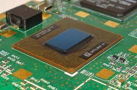
The semiconductor manufacturing ecosystem is locked in an intense race to optimize structural packing efficiency as modern industrial applications demand a seamless blend of hyper-connectivity and energy efficiency. Traditional monolithically designed integrated circuits are rapidly giving way to modular, heterogeneous integration strategies where distinct functional chiplets are stitched together within a single high-performance package. This modular approach relies heavily on advanced micro-bumping and face-down die attachments to establish the high-density interconnect grids needed for disparate processing units to communicate with near-zero latency. The resulting performance leap is empowering automotive manufacturers to install highly responsive autonomous driving computers, while enabling telecommunications providers to roll out ultra-reliable infrastructure networks. As global industries increasingly transition toward completely cloud-dependent operational models, the baseline hardware infrastructure must undergo a permanent, high-velocity modernization cycle. Corporate strategists keeping a watchful eye on a detailed Flip Chip Technology Market forecast can gain invaluable insights into shifting component lead times, material cost curves, and emerging assembly standards worldwide.
Simultaneously, the widespread commercialization of wearable medical diagnostics and internet-of-things devices is opening up highly lucrative frontiers for specialized, ultra-thin packaging solutions that require minimal power consumption. These miniaturized applications demand specialized bumping alternatives, such as gold and continuous copper pillars, which provide the structural rigidity and fine pitch scaling necessary to fit into flexible, low-profile product housings. This expansion beyond traditional heavy computing environments highlights the incredibly versatile nature of face-down assembly mechanics and its unique ability to solve geometric design constraints across highly diverse product lines. On an environmental front, the manufacturing sector is actively grappling with strict international regulations aimed at eliminating lead and hazardous chemical substances from electronic assemblies, driving heavy research into eco-friendly solder alternatives and halogen-free underfill materials. This green electronics movement is fast becoming a core competitive differentiator as corporate sustainability benchmarks become legally binding across major consumer markets. As regional technology clusters strive to build self-sustaining component ecosystems, the cross-pollination of material science and automated assembly robotics will undoubtedly fuel a highly dynamic era of low-cost, ultra-reliable hardware integration.
How do copper pillar bumps differ from standard spherical solder bumps in advanced packaging? Copper pillar bumps consist of a solid copper cylinder topped with a small cap of lead-free solder, whereas traditional bumps are entirely spherical solder structures. The rigid cylindrical geometry of copper pillars prevents the solder from collapsing or bridging during assembly, allowing for much finer interconnect pitches, higher current densities, and enhanced thermal performance.
What role does this packaging method play in the modern development of modular chiplet architectures? Modular chiplet architectures require multiple independent silicon dies to communicate at extremely high speeds with minimal latency within a single substrate housing. This face-down packaging method provides the massive density of microscopic I/O connections necessary to link these chiplets together tightly, effectively mimicking the performance of a single large, expensive monolithic chip.
➤➤➤Explore MRFR’s Related Ongoing Coverage In Semiconductor Industry:
Restaurant Delivery Robot Market
Ground Penetrating Radar Market